AZSA-DefectNavi

Overview
Our cutting-edge system empowers you to thoroughly analyze the factors impacting semiconductor wafer yield by capturing and integrating defect information from advanced inspection equipment. This powerful tool enables precise visualization of defect locations on semiconductor wafers and offers sophisticated classification capabilities, ensuring you can identify and address yield issues with unmatched accuracy.
Features
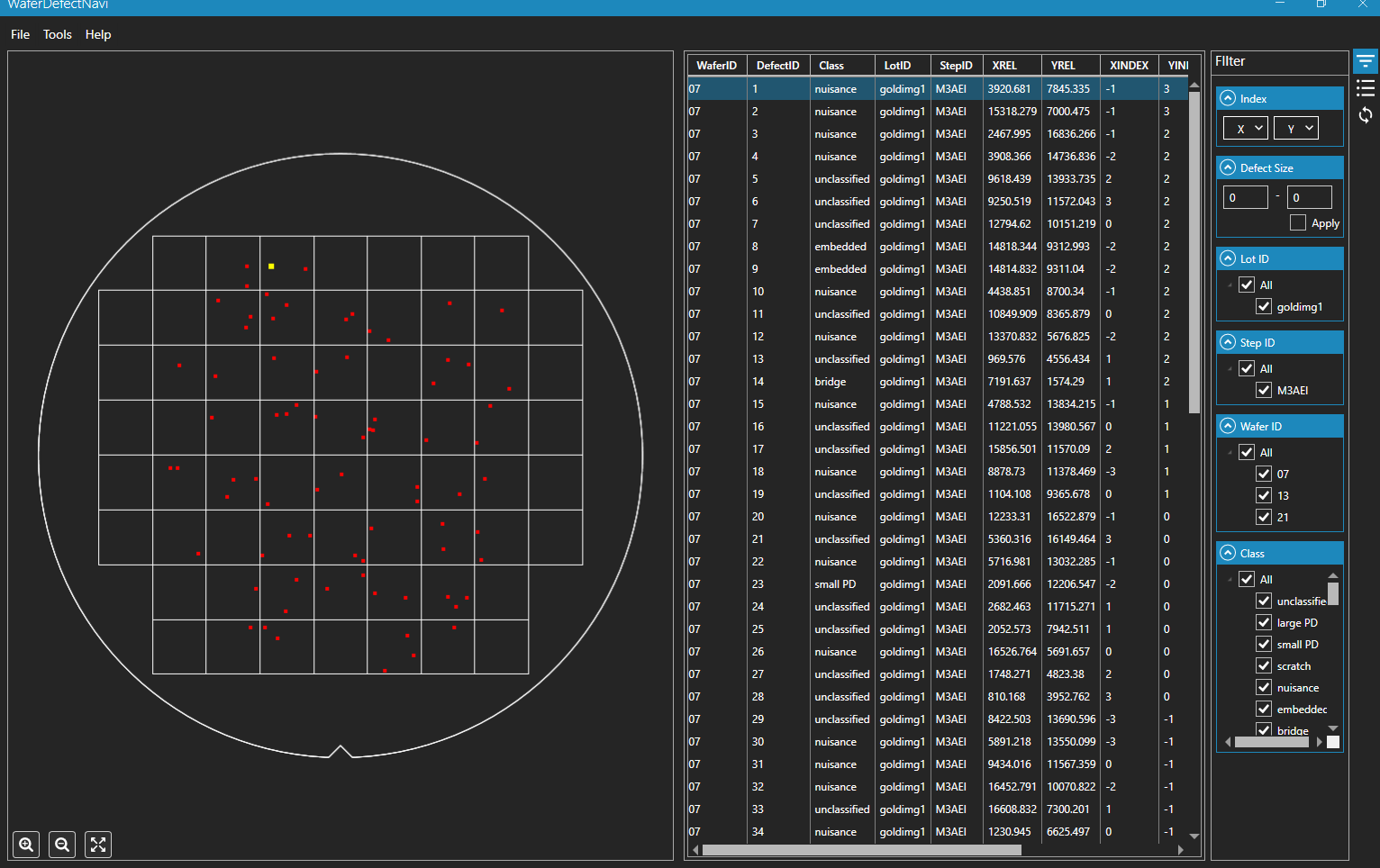
- Seamlessly integrate defect data from the inspection system, accurately mapping defect locations on the wafer with detailed, comprehensive information for each identified defect.
- Visualize defect distribution effortlessly with our advanced wafer map, enabling you to gain clear insights into potential yield issues.
- Efficiently manage multiple wafers by importing and displaying defect data across various wafers, ensuring thorough analysis and comparison.
- Refine your analysis by focusing on specific areas of the wafer, allowing you to narrow down defect distribution with precision.
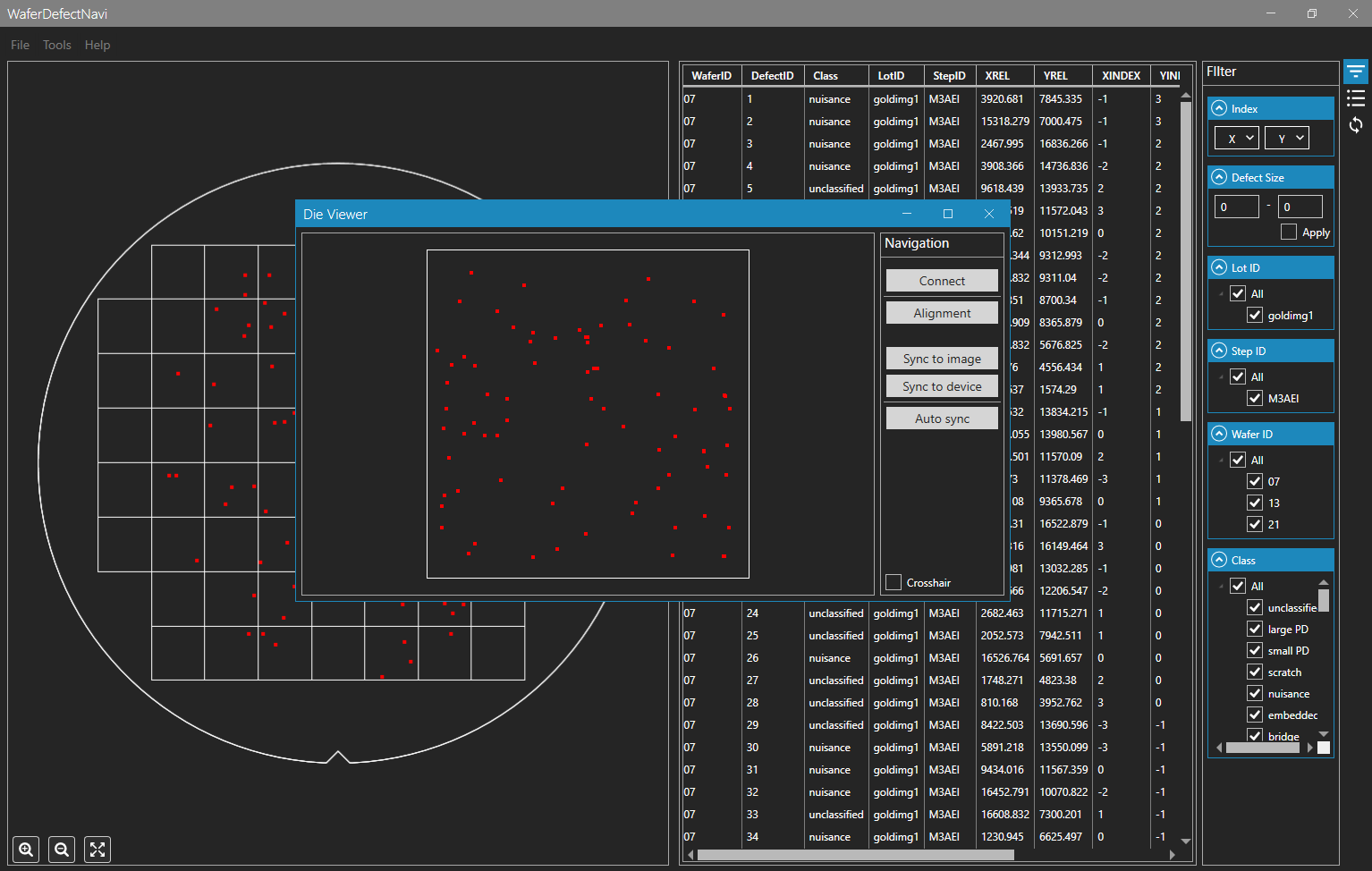
- Target specific dies with ease, displaying the exact distribution of defects within the selected die for more detailed examination.
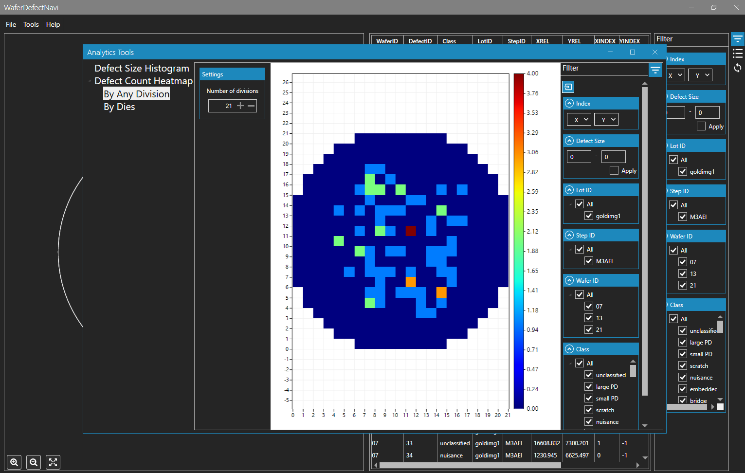
- Generate insightful histograms for defect sizes, providing you with a visual representation of defect characteristics at a glance.
- Create precise heat maps by dividing the wafer into customizable sections, offering a clear view of defect concentration and helping to identify critical areas for further investigation.
- By editing the data, you can output only the necessary defect information for analysis.


